Advanced SEM/EDS technology.
SCANNING ELECTRON MICROSCOPY (SEM) AND ENERGY DISPERSIVE X-RAY SPECTROSCOPY (EDS).
Scanning Electron Microscopy (SEM) and Energy Dispersive X-Ray Spectroscopy (EDS) with full digital imaging has emerged as an essential tool in metallurgical testing and failure analysis. Using a beam of highly energetic electrons, SEM allows us to acquire live, high-resolution, micro scale, three-dimensional images of the surface of a failed metal part or component. Using these digital images with a magnification of up to 500,000x, we are able to study the fracture topography and morphological characteristics of the failed metal part or component to determine the failure mode and root cause. Scanning electron microscopy with EDS is also used for determining the chemical composition of constituents in the microstructure, determining plating types, finding and chemically analyzing contamination, and more.
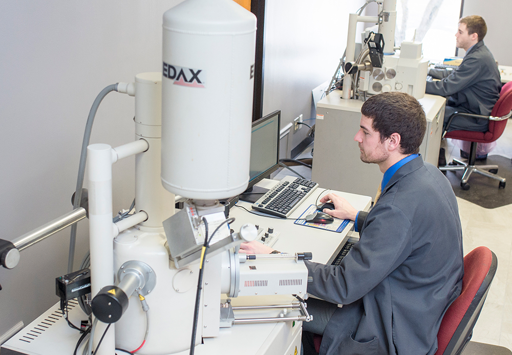
At ATRONA we have two full SEM/EDS systems. One of these systems features cutting-edge technology in the field of microscopy giving us an advantage with clear imaging and EDS mapping capabilities. The other SEM was upgraded with new software and controls. One of our SEM's is capable of variable pressure allowing us to perform analysis on plastics and all non-conductive materials.
ATRONA'S SEM Capabilities include:
- Revolutionary automatic alignment functions; auto beam setting, auto aperture, etc.
- Better resolution of any of its kind due to new electron optics
- Real time full screen image, dual image and signal mixing
- Newly developed high sensitivity solid state type BSE detector
- Computer eucentric, 5-axis motorized stage with motorized tilt
- Can accommodate sample as tall as 85 mm for elemental analysis without cutting
- Analytical specimen chamber with optimum geometry for simultaneous accommodation of EDS
- Variable pressure allows observations of wet, oily, and non conductive samples (polymers)
EDAX Full Energy Dispersive X-Ray Spectroscopy Capabilities:
- Qualitative analysis
- Quantitative analysis
- Elemental Mapping and Scanning
- Fast and Accurate plots of elemental distributions
- Powerful automated particle analysis
- Automated spectrum collection
Evaluating Failure Mode with SEM
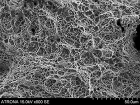
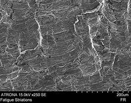
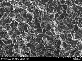
SEM allows us to acquire live, high-resolution, micro scale, three-dimensional images of the surface of a failed metal part or component. Using these digital images or "photomicrographs" with a magnification of up to 500,000x, failure modes are easily revealed and identified. Even if the fracture face is corroded or has other contamination, ATRONA has ways to clean the fracture surface to reveal the mode of failure. Fracture initiation can also be revealed.
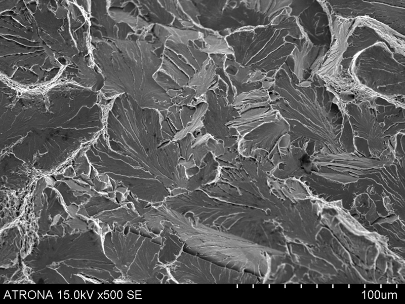
Dimple Rupture 800x
Fatigue Striations
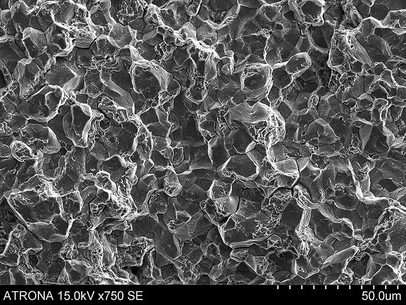
Intergranular Failure Mode
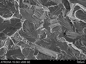
Cleavage 500x
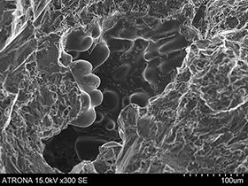
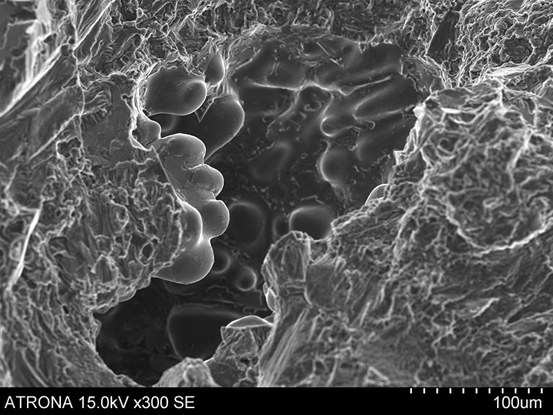
Solidification Shrinkage Porosity
Generally speaking, failure modes are either ductile or brittle. Ductile failures are typically accompanied by significant plastic deformation. Brittle failures are normally accompanied by no elongation or plastic deformation. They produce catastrophic failures with little to no strain. Ductile fractures are more desirable than brittle fractures because generally ductile fractures give warnings prior to a catastrophic event.
Specific failure modes include Dimple Rupture Overload, Microvoid Coalescence, Intergranular and Transgranular, Stress Corrosion Cracking, Hydrogen Embrittlement, Gaping Grain Boundaries, Cleavage Rupture, Creep and Elongation, Tensile and Compressive Modes, Corrosion (various types), Fatigue (High and Low Cycles & High and Low Loads), Lamination and Streaking, Embrittlement, and others.